

Basic knowledge of FPC circuit board
- Categories:Company News
- Author:
- Origin:
- Time of issue:2021-03-08
- Views:
(Summary description)With the continuous increase in the yield ratio of flexible PCBs and the application and promotion of rigid-flex PCBs, it is now more common to add soft, rigid or rigid-flex when talking about PCBs, and say that it is a few-layer FPC. Generally, an FPC made of a soft insulating substrate is called a soft FPC or a flexible FPC, and a rigid-flex composite PCB is called a rigid-flex PCB. It meets the needs of today's electronic products for high density, high reliability, small scale, and lightweight progress. It also satisfies the strict economic requirements and the needs of market and technology competition.

Basic knowledge of FPC circuit board
(Summary description)With the continuous increase in the yield ratio of flexible PCBs and the application and promotion of rigid-flex PCBs, it is now more common to add soft, rigid or rigid-flex when talking about PCBs, and say that it is a few-layer FPC. Generally, an FPC made of a soft insulating substrate is called a soft FPC or a flexible FPC, and a rigid-flex composite PCB is called a rigid-flex PCB. It meets the needs of today's electronic products for high density, high reliability, small scale, and lightweight progress. It also satisfies the strict economic requirements and the needs of market and technology competition.
- Categories:Company News
- Author:
- Origin:
- Time of issue:2021-03-08
- Views:
With the continuous increase in the yield ratio of flexible PCBs and the application and promotion of rigid-flex PCBs, it is now more common to add soft, rigid or rigid-flex when talking about PCBs, and say that it is a few-layer FPC. Generally, an FPC made of a soft insulating substrate is called a soft FPC or a flexible FPC, and a rigid-flex composite PCB is called a rigid-flex PCB. It meets the needs of today's electronic products for high density, high reliability, small scale, and lightweight progress. It also satisfies the strict economic requirements and the needs of market and technology competition.
Overseas, flexible PCB has been widely used in the early sixties. In my country, it was only in the sixties that it started production and application. In recent years, as the world’s economic integration and the opening up of the market, the amount of technology introduced has been continuously increasing. Some small and medium-sized rigid FPC factories have used soft and hard work skills to take advantage of the existing opportunities. The facility implements improvements to tooling tools and processes, transforming the production of flexible PCBs and adapting to the ever-increasing demand for flexible PCBs. In order to further understand the PCB, this section will give a research and discussion introduction to the soft PCB process.
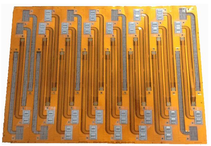
One, flexible PCB classification and its advantages and disadvantages
1. Flexible PCB classification
Flexible PCBs are generally classified as follows according to the number and structure of conductors:
1.1 Single-sided flexible PCB
Single-sided flexible PCB has only one layer of conductor, and the surface can have a covering layer or no covering layer. The insulating base material used varies with the application of the product. Commonly used insulating materials include polyester, polyimide, polytetrafluoroethylene, and soft epoxy-glass cloth.
Single-sided flexible PCB can be further divided into the following four categories:
1) One-sided co-signed without covering layer
The conductor pattern of this kind of flexible PCB is on the insulating substrate, and the conductor has no covering layer on the outside. It is the same as a general single-sided rigid FPC. This type of product is the cheapest one, and is generally used in non-critical and background-oriented applications. The interconnection is successfully realized by soldering, welding or pressure welding. It is commonly used in early telephones.
2) One-sided co-signed with a cover layer
This type is similar to the previous type, but an extra layer of covering layer is added to the surface of the wire according to customer requirements. The pads should be exposed when covering, and it can simply be left uncovered in the end area. If accuracy is required, the clearance hole method can be used as appropriate. It is the most widely used and widely used single-sided flexible PCB. It is widely used in transportation instrumentation and electronic spectrograph.
3) Double-sided co-signed without covering layer
This type of connection disk interface can be connected on the front and back of the wire. In order to achieve this, a via hole is opened in the insulating substrate at the pad. This via hole can be punched, etched or made by other mechanical methods at the required position of the insulating substrate. It is used for mounting elements, components and soldering on both sides. There is no insulating substrate in the pad area of the via. Such pad area is generally removed by chemical means.
4) Double-sided co-signed with a cover layer
The difference between this type and the previous type is that there is a covering layer on the outside. However, the covering layer has via holes, and it is allowed to be terminated on both sides, and the covering layer is still maintained. This kind of flexible PCB is made of two layers of insulating materials and a layer of metal conductors. It is used when the covering layer and the surrounding devices are insulated from each other, and they need to be insulated from each other, and the ends need to be signed on both the front and back sides.
1.2 Double-sided flexible PCB
Double-sided flexible PCB with two layers of conductors. The application and advantages of this type of double-sided flexible PCB are the same as those of single-sided flexible PCB. Its main advantage is to increase the density of wiring per unit plane or surface size. It can be divided into with or without metallized holes and with or without covering layer: a without metallized holes, without covering layer; b without metallized holes, with covering layer; c with metallized holes, without covering layer ; d There are metallized holes and covering layers. Double-sided flexible PCBs without covering layers are rarely used.
1.3 layer flexible PCB
Flexible multi-layer PCB is like rigid multi-layer PCB, it can be made into multi-layer FPC flexible circuit board by using multi-layer lamination technology if deemed appropriate. The simplest multilayer flexible PCB is a three-layer flexible PCB formed by covering two copper shielding layers on both sides of a single-sided PCB. This kind of three-layer flexible PCB is better than my own in terms of electrical characteristics, and looks better as a coaxial wire or shielded wire. The most commonly used multi-layer flexible PCB structure is a four-layer structure, which uses metallized holes to successfully achieve inter-layer interconnection. The half mid-waist two layers are generally the power layer and the ground layer.
The advantage of multilayer flexible PCB is that the base film is light in weight and has good electrical special properties, such as low dielectric constant. The multi-layer flexible PCB board made of polyimide film as the base material is about 1/3 lighter than the rigid epoxy glass cloth multi-layer PCB board, but it misses the single-sided and double-sided flexible PCB. Good flexibility, most of these products do not require flexibility.
Multilayer flexible PCB can be further divided into the following types:
1) A multilayer PCB is formed on a flexible insulating substrate, and the finished product is stipulated to be flexible: this structure generally bonds the two sides of a lot of single-sided or double-sided microstrip flexible PCBs together, but that The inner core part is not glued together, so it has a high degree of flexibility. In order to have the desired electrical special properties, such as the special properties and impedance performance that match the rigid PCB to which it is interconnected, each circuit layer of the multilayer flexible PCB device must be preset with signal lines on the ground plane. In order to have a high degree of flexibility, a thin, adaptable coating, such as polyimide, can be used on the wire layer to replace a thicker laminated covering layer. The metallized holes enable the z-plane between the flexible circuit layers to successfully achieve the required interconnection. This multilayer flexible PCB is most suitable for use in presets that require flexibility, high reliability, and high density.
2) A multilayer PCB is formed on a flexible insulating substrate, and the finished product is not specified to be flexible: This type of multilayer flexible PCB is made of a soft insulating material, such as polyimide film, and the layers are restrained into a multilayer board. The inherent flexibility was missed after lamination. When the special properties of the insulation of the film, such as low dielectric constant, average thickness of the medium, lighter weight, and continuous processing, are used in the predetermined upper limit, it is considered appropriate to use this kind of flexible PCB. For example, a multilayer PCB made of polyimide film insulating material is about one-third lighter than a rigid PCB with epoxy glass cloth.
3) A multilayer PCB is formed on a flexible insulating substrate, and the finished product must be shapeable, rather than flexible: this type of multilayer flexible PCB is made of flexible insulating materials. Although it is made of soft materials, it is limited by electrical presets. For example, for the required conductor resistance, a thick conductor is required, or for the required impedance or capacitance, there is a requirement between the signal layer and the ground layer. Thick insulation isolation, because of this, it is already formed in the finished application. The technical term "formable" is defined as: multilayer flexible PCB devices have experience in making the required patterns, and can no longer be flexed in the application. It is used in the wiring in the avionics unit. At this time, it is required that the strip line or three-dimensional space preset conductor resistance is low, capacitive coupling or circuit noise is extremely small, and the interconnection end can be flexed to 90° flat and smooth. Multi-layer flexible PCB made of polyimide film material successfully realized the work of this kind of wiring. Because the polyimide film has high temperature resistance, flexibility, and the overall electrical and mechanical special properties are satisfactory. In order to successfully realize all the interconnections of the device profile, the traces therein can be further divided into multiple multi-layer flexible circuit devices and pieced together with adhesive tape to form a printed circuit bundle.
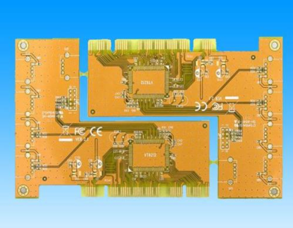
1.4 rigid-flexible multilayer PCB
This type is generally on one or two rigid PCBs, which contain the soft PCB necessary to form a group. The flexible PCB layer is laminated in the rigid multi-layer PCB. This is to meet special electrical requirements or to extend outside the rigid circuit. It has experience in the simplest surface circuit installation of the dynasty Z. This type of product has been widely used in electronic facilities that take compression weight and size as the key, and must ensure high reliability, high density assembly, and good electrical and special properties.
Rigid-flexible multi-layer PCBs can also hold the ends of many single-sided or double-sided flexible PCBs together to become rigid parts, while the half-waist non-adhesive becomes soft parts, and the rigid part of the Z-side is used Metallized via interconnection. The flexible circuit can be laminated into the rigid multi-layer board. This type of PCB is increasingly used in those occasions that require ultra-high packaging density, good electrical special properties, high reliability, and strict size limitations.
There have been a series of mixed multilayer flexible PCB devices preset for use in military avionics facilities. In these applications, weight and size are critical. In order to meet the specified weight and size limits, the density of the inner packaging must be extremely high. In addition to the high degree of open circuit density, in order to minimize crosstalk and noise, all signal transmission lines must be shielded. If you want to use shielded clutch wires, it is actually impossible to economically package them into the system. In this way, a mixed multi-layer
Flexible PCB to successfully realize its interconnection. This device contains the shielded signal line in the flat stripline flexible PCB, and then it is an indispensable part of the rigid PCB. In a relatively high-level operating situation, after the production is completed, the PCB forms a 90° S-shaped buckling, so it provides the simplest surface interconnection path for z, and under the simplest surface oscillation stress effect of x, y and z , Can eliminate the stress-strain on the solder joints.
2. Strengths Rigid area range Rigid area range
2.1 Flexibility
A significant advantage of using flexible FPC is that it can be more convenient to wire and install in three-dimensional space, and it can also be rolled or folded for use. As long as it is curled within the allowable radius of curvature, it can withstand thousands to tens of thousands of applications without being destroyed.
2.2 Reduce size
In the assembly and connection of components, the conductor section of the flexible PCB is thin and flat compared with the use of conductive cables, which reduces the size of the conductors and can be formed along the casing, making the structure of the facility more compact and reasonable, and smaller Even the size of the outfit. Compared with rigid PCB, space can be saved by 60~90%.
2.3 Reduce weight
Within the same size, the weight of a flexible PCB can be reduced by about 70% compared with a wire and cable at the same current carrying capacity. Compared with a rigid PCB, the weight can be reduced by about 90%.
2.4 installations are exactly the same
The flexible PCB is used to install the connection, which eliminates the error when wiring with wires and cables. As long as the processing drawings are corrected, all the winding circuits produced later will be the same. There will be no wrong connection when installing the connection line.
2.5 increases reliability
When it is deemed appropriate to use a flexible PCB assembly connection, because it can be wired on the three simplest planes of X, Y, and Z, the transfer interconnection is reduced, the reliability of the entire system is increased, and the fault is investigated. Provide convenience.
2.6 Preset controllability of electrical parameters
According to the application requirements, the designer can control capacitance, inductance, special impedance, delay and attenuation when implementing flexible PCB presets. It can be preset to have the special nature of the mission conveying line. Since these parameters are related to wire width, thickness, spacing, insulating layer thickness, dielectric constant, damage angle tangent, etc., it is not easy to do when using wire cables as appropriate.
2.7 ends can be group soldered
Flexible PCB, like rigid PCB, has terminal pads, which can eliminate wire stripping and tinning, thus saving costs. Terminal pads are connected to elements, components, and plugs, and dip soldering or wave soldering can be used to replace the manual soldering of each wire.
2.8 Material use can be selected
Flexible PCB can be made with different base materials according to different application requirements. For example, polyester film can be used in assembly applications that require low cost. In demanding applications, good performance is required, and polyimide film can be used.
2.9 low cost
Use flexible PCB to install the connection, which can reduce the total cost. This is because:
1) Because the various parameters of the wires of the flexible PCB are exactly the same; the implementation of group termination eliminates the incorrect and rework often occurring in the cable guide and connection, and the modification of the flexible PCB is more convenient.
2) The application of flexible PCB simplifies the structure preset, it can be directly pasted to the component, reducing the damage of the clamp and its fixing parts.
3) For wires that require shielding, flexible PCBs are cheaper.
2.10 Continuous processing
Because the flexible foil-clad laminate can be supplied continuously in roll form, because this can successfully realize the continuous production of FPC closed doors. This also helps reduce costs.
3. Lack
3.1 One-time high initial cost
Because the flexible PCB is preset and manufactured for special applications, the initial circuit setup, wiring, and photographic film require a higher cost. It is wrong to use flexible PCBs for special needs. Generally, it is best not to use them for small-scale applications.
3.2 It is difficult to change and patch the flexible PCB
Once the flexible PCB is manufactured, it must be changed from the base map or knitting procedure, because this is not easy to change. The outer surface is covered with a layer of film that takes care of it as much as possible. It must be removed before patching, and it needs to be restored after patching. This is a relatively difficult office.
3.3 size limitation only
Flexible PCBs are generally manufactured by batch process under uncommon conditions. Because of the limitation of the size of the production facility, they cannot be made very long and wide.
3.4 The operation is inappropriate and easily destroyed
The operation of the person in charge of the installation is not suitable for the destruction of the flexible circuit, and the soldering and reworking need to be operated by the person in charge of training.
Scan the QR code to read on your phone
-
 Basic knowledge of FPC circuit board
With the continuous increase in the yield ratio of flexible PCBs and the application and promotion of rigid-flex PCBs, it is now more common to add soft, rigid or rigid-flex when talking about PCBs, and say that it is a few-layer FPC. Generally, an FPC made of a soft insulating substrate is called a soft FPC or a flexible FPC, and a rigid-flex composite PCB is called a rigid-flex PCB. It meets the needs of today's electronic products for high density, high reliability, small scale, and lightweight progress. It also satisfies the strict economic requirements and the needs of market and technology competition. - Fpc flexible circuit board test method and standard 03-08
- Interpretation of four-layer PCB circuit board stack design scheme 03-08
- What are the common rules for PCB wiring? 03-08
- PCB assembly quality and reliability control of electroless nickel-palladium-gold plating 03-08

Service Hotline:
Email:lhdpcb@vip.163.com
Address:No. 26, Meiyuan 3rd Road, Intercontinental Industrial Park, Luoyang Town, Boluo County, Huizhou
 0752-6260118

 QQ
QQ 

Copyright ©Huizhou Linghangda Technology Co., Ltd. All Rights Reserved 粤ICP备18145577号
Power by: www.300.cn