

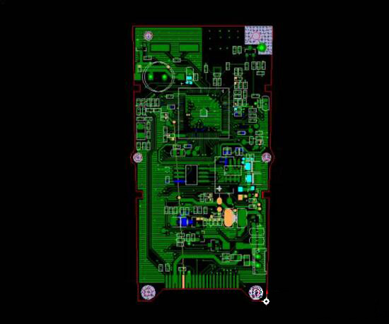
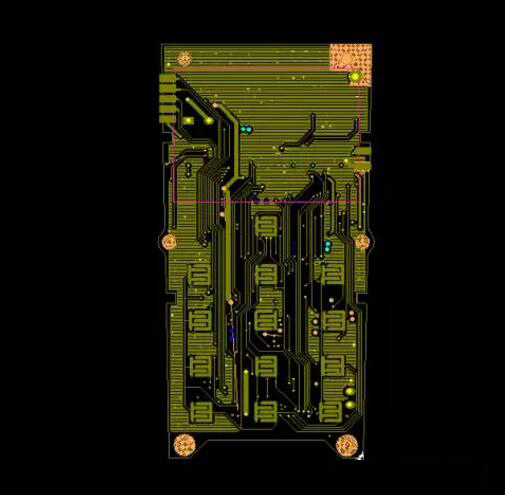
Interpretation of four-layer PCB circuit board stack design scheme
- Categories:Company News
- Author:
- Origin:
- Time of issue:2021-03-08
- Views:
(Summary description)When imagining a four-layer PCB circuit board, how to imagine that the stack is normal? In practice, there can be three plans. Plan one, 1 power layer, 1 floor, and 2 signal layers. Discrimination is displayed like this: TOP (signal layer), L2 (floor), L3 (power layer), BOT (signal layer). Plan two, 1 power layer, 1 floor, and 2 signal layers. The identification is displayed like this: TOP (power layer), L2 (signal layer), L3 (signal layer), BOT (floor). Plan three, 1 power layer, 1 floor, and 2 signal layers. Discrimination is displayed like this: TO

Interpretation of four-layer PCB circuit board stack design scheme
(Summary description)When imagining a four-layer PCB circuit board, how to imagine that the stack is normal?
In practice, there can be three plans.
Plan one, 1 power layer, 1 floor, and 2 signal layers. Discrimination is displayed like this: TOP (signal layer), L2 (floor), L3 (power layer), BOT (signal layer).
Plan two, 1 power layer, 1 floor, and 2 signal layers. The identification is displayed like this: TOP (power layer), L2 (signal layer), L3 (signal layer), BOT (floor).
Plan three, 1 power layer, 1 floor, and 2 signal layers. Discrimination is displayed like this: TO
- Categories:Company News
- Author:
- Origin:
- Time of issue:2021-03-08
- Views:
When imagining a four-layer PCB circuit board, how to imagine that the stack is normal?
In practice, there can be three plans.
Plan one, 1 power layer, 1 floor, and 2 signal layers. Discrimination is displayed like this: TOP (signal layer), L2 (floor), L3 (power layer), BOT (signal layer).
Plan two, 1 power layer, 1 floor, and 2 signal layers. The identification is displayed like this: TOP (power layer), L2 (signal layer), L3 (signal layer), BOT (floor).
Plan three, 1 power layer, 1 floor, and 2 signal layers. Discrimination is displayed like this: TOP (signal layer), L2 (power layer), L3 (floor), BOT (signal layer).
Signal layer

Strata
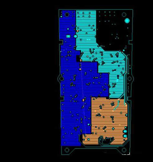
Power layer
Signal layer
What are the advantages and disadvantages of these three plans?
Plan 1. The main laminate design plan of the four-layer PCB of this plan is that there is a three-dimensional under the component surface, and the key signal preselects the TOP layer; as for the layer thickness installation, there are the following suggestions:
Satisfying that the impedance control core board (GND to POWER) should not be too thick to increase the three-dimensional dispersion impedance of the power supply and ground; to ensure the three-dimensional decoupling effect of the power supply.
Scheme two, some schemes mainly in order to achieve a certain shielding effect, put the power supply and ground plane on the TOP and BOTTOM layer, but this scheme must achieve the ideal shielding effect, at least the following defects: 1. The power supply and the ground are too far apart, the power supply The plane impedance is large. 2. The power supply and ground plane are extremely incomplete due to the influence of component pads. Because the reference plane is incomplete and the signal impedance is not continuous, in fact, due to the large number of surface mount devices, the power supply and ground of this solution can hardly be used as a complete reference plane, and the expected shielding effect is very high when the devices are getting denser. Difficult to achieve; Solution 2 has a limited range of use. But among individual boards, Solution 2 is the best layer setting solution.
Scheme 3: This scheme is similar to scheme 1, and is suitable for the case where the main components are laid out in the BOTTOM layout or the bottom layer of key signals;
Scan the QR code to read on your phone
-
 Basic knowledge of FPC circuit board
With the continuous increase in the yield ratio of flexible PCBs and the application and promotion of rigid-flex PCBs, it is now more common to add soft, rigid or rigid-flex when talking about PCBs, and say that it is a few-layer FPC. Generally, an FPC made of a soft insulating substrate is called a soft FPC or a flexible FPC, and a rigid-flex composite PCB is called a rigid-flex PCB. It meets the needs of today's electronic products for high density, high reliability, small scale, and lightweight progress. It also satisfies the strict economic requirements and the needs of market and technology competition. - Fpc flexible circuit board test method and standard 03-08
- Interpretation of four-layer PCB circuit board stack design scheme 03-08
- What are the common rules for PCB wiring? 03-08
- PCB assembly quality and reliability control of electroless nickel-palladium-gold plating 03-08

Service Hotline:
Email:lhdpcb@vip.163.com
Address:No. 26, Meiyuan 3rd Road, Intercontinental Industrial Park, Luoyang Town, Boluo County, Huizhou
 0752-6260118

 QQ
QQ 

Copyright ©Huizhou Linghangda Technology Co., Ltd. All Rights Reserved 粤ICP备18145577号
Power by: www.300.cn